A step by step description of the Circuit
A few words to start with. In this section, I will describe the technical what and why and give some background on the circuits. This will
help understanding the full DDDAC1794 NOS document (click here)
and as well give some insight in the functioning of the DAC
It is all the technical stuff, feel free to skip it...
You can actually click on the circuits and get a pretty detailed version back. Nice for the 2 Monitor users :-)
(or push the button below:)


Block Diagram
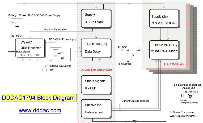
The main functionality is shown in the block diagram. The USB connection
comes through the WaveIO USB receiver. The I2S Signals are connected to the
outside world by an optocoupler. Therefore no galvanic connections
should
be made between DAC and USB. Hence the separate 5 Volt power supply (or use
BUS Power mode). The 3.3V supply for the optocoupler comes from the
Mainboard and is well filtered to obtain low jitter I2S signals.
On the Mainboard the I2S Data from the WaveIO board (or external...) is
led directly to the I2S - right-justified (RJ) converter. Which is built up
from 5 times the 74VHC164 shift registers to get the 7 clock cycles delay for the right
channel and (32+7) 39 clock cycles for the left channel. This section is also
supplied by the same 3.3 Volt supply which feeds the optocoupler delivering
the I2S signals.
The RJ signals now go to the actual DAC module. Each board has 2 PCM1794A
chips which work in NOS mono mode. The chips are being powered by 3.3V for
the digital section and with 8.0V for the analog section. Right and left
channels are completely separated.
The PCM1794 has balanced current outputs. These are fed back to the
Mainboard, effectively added when parallel boards are being used. Here
the passive I/V conversion takes place and the signal is being taken directly
from the resistor to minimize any negative effects from long wires.
The generated signal can be decoupled to the analog output connector in
single mode by use of a single capacitor. I suggest 2,2uF. When a
transformer is being used, two options are possible. Completely balanced
output or balanced to single ended (I did this with the Sowter transformer).
The latter reduces the d2 distortion component in the signal and allows for
extra gain.

Mainboard
The heart of the Mainboard is the delay section around the 5x 74VHC164
(IC2-6) 8 bit shift registers. I choose to not use resistors in between to avoid
any data signal delays. The 3.3V supply is built up with IC1 the LF33. I used
Nichicon audio grade capacitors C1 and C3 to buffer / filter the power lines.
The 10 position pin headers are used for easy connection with the WaveIO Board.
Please note this is a proprietary design, so not according to any standard. The
LED signal section is on the main board, but is completely isolated from the
other electronics. The WaveIO board is driving the LEDs with 8mA current
sources. So any LED can be used, color and light intensity are not relevant.
There are LEDs for the sample frequency (Fs = 44.1, 48, 88, 96, 176 and 192
kHz), Host active and Audio stream. Very helpful indications!
The current outputs from the DAC are summed up on the Mainboard. In the
Mono Mode, actually the two DACs inside the chip are already operating in parallel, so the
outputs can be tied up together to sum up the currents. For the passive I/V conversion, which is done by the parallel of Ra // Rb,
space is offered for these two resistors. By using two resistors, you can combine to different values. With one deck,
270 Ohm per current output is the nominal load. There are two current outputs parallel, so one 133 Ohm resistor
is being used. The small table at top right shows the values when more than one DAC module is being used.
In the circuit the single ended output is connected to the positive (POS)
output, but it is totally irrelevant which one is used. Feel free to use the
negative output (NEG). The 100k resistor is just the bleeder for the output
capacitor. This might be higher or lower, but 100k is a good compromise
between many arguments. The C9-10 are here 2.2uF, but value is not
critical. It depends on your load of the following stages input impedance
and the required lowest frequency at -3dB (so here that is approximately 1Hz).

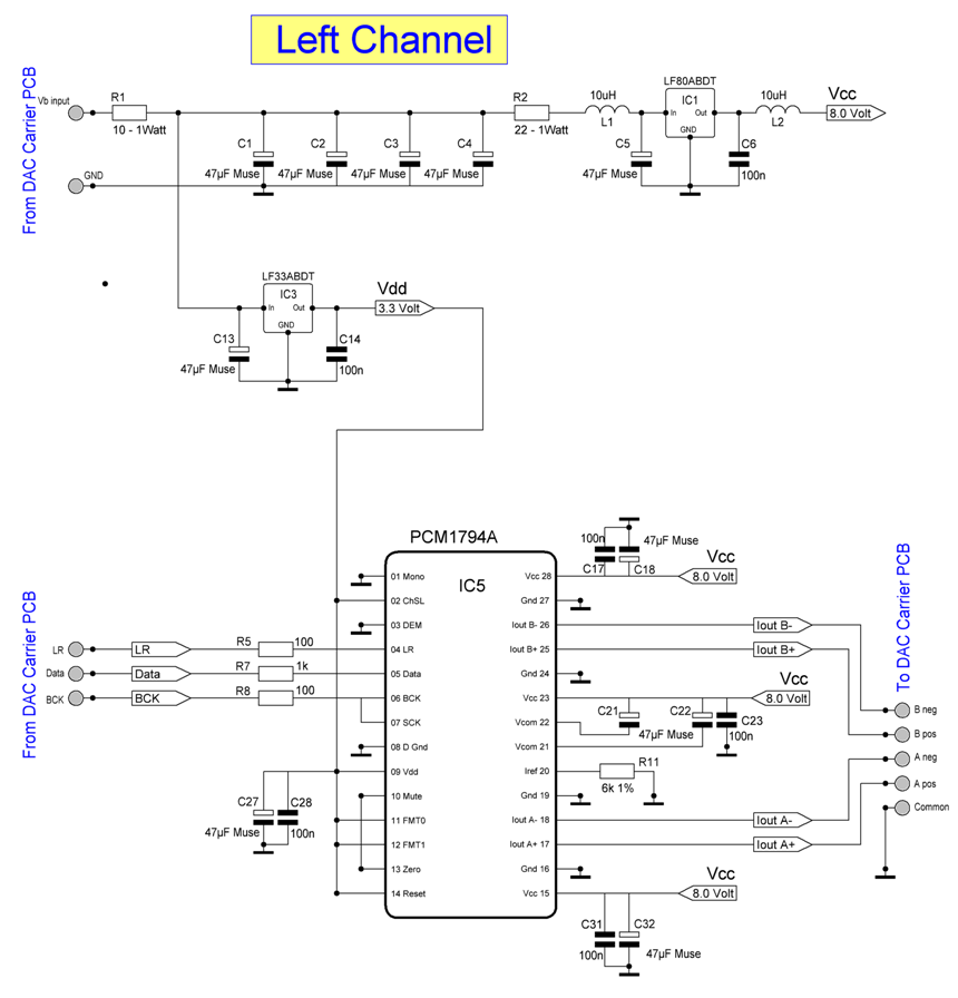
DAC Module (one Channel shown)
As both channels are 100% identical, I only describe one. The key to success
is the local power supply and its filtering. Every board is fed by the master
12V supply and it is important that at the entrance of the PCB there is already
first decoupling. This is done with R1 and C1-4. By doing this we almost present
an independent supply to every board and hence every DAC chip. From this point
the power splits up in a digital part and an analog part. The digital part is
straight forward with the LF33 close to the DAC chip. The regulator needs some
cooling, which is done automatically due to the SMD assembly. The PCB is kind of
the cooling for the chip (why it is black). The analog section round IC1,
the LF80 is being decoupled at input and output with a LC network. The value are
chosen such, that the transfer characteristic is relatively slow and has no
overshoot. Do not change these values.
The connections round PCM1794 are a bit special. So far I have seen
almost every 1794 design in the internet simply based 1:1 on the datasheet.
Clearly no one made some thoughts here. Read my Design section for more
detail. The inputs are connected through the decouple resistors R5-7. R6 is
1kOhm to add some extra delay, to compensate for the extra 1/2 clock cycle
in the delay section due to the VHC164 clock function. Pin 6 and 7 (BCK and
SCK) are both connected to the BCK. This is THE GREAT TRICK to make the
PCM1794 actually work in NOS mode (against all datasheet guidance ;-) The
analog section is nothing else than 4 current sources supplying the analog
signal. Therefore there is audio grade decoupling of all voltage connections.
The bias pin 20 called Iref, delivers 2,4 Volt and by the value of R11
generates a current which is used through mirroring inside the chip as
reference. The datasheet has NO INFORMATION AT ALL how this works, but gives
10k as guidance. By measuring and combining, the optimum solution for output
voltage and maximum headroom (so minimum distortion) turned out to be 6k1
(R11)...
The actual current outputs are balanced and two fold (as a stereo chip is
used in mono). The currents are led towards the Mainboard where the summing
of all DACs is done at a single point (the I/V resistor) and the resulting
VOLTAGE is picked directly from the pins of that resistor. Therefore it is
no problem at all, that the leads are longer and the summing of current take
place between the decks.

Power Supply ( for 5 Volt and for 12 Volt)
The (interesting) story behind this power supply design and how it came to
this version, is described in its own section. Right here, I will only describe
how it actually works. A few words up front; the design is quite universal and
can be used for many other voltages and power ranges. Keep in mind it needs
roughly 6 Volts more input than output... Within some reasonable ranges It is
just a matter of size of the transformer and heat sinks. Warning: there is NO
overload or short circuit protection. Nor is there a thermal protection. For
safety there is a fuse and that's it. All under the motto, less is better ;-) A
little care with the handling of this supply is therefore needed. Most
important, it sounds really great!
As every power supply, it starts with rectifying and basic filtering to
generate a rough DC voltage which is than being regulated by use of a series
element (here a transistor Darlington TIP122). In my Jean Hiraga Le Monstre
based amplifiers and the TUMOS design, I already had good experience using RC filters in the first stage. So also here we start with a double RC
filter R1-C1 and R2-C2 after the actual rectifying by the double
Schottky D1 diodes. This voltage is being regulated by Dar1 and goes through
R6 straight to the output. Which is decoupled by C7-9
We will work our way back in the circuit... The center tab from P1
(setting the output DC voltage) is lead to the base of T3 and this
voltage is being compared with the voltage over LED2. This voltage is
quite constant as it is being sourced by the regulated output voltage
and R8. The difference (called error) is now being amplified by T3,
which works as a common emitter amplifier. This error-correction-signal
is going to the basis of T2, which is nothing less than an extra driver
for the Darlington, reducing control current to almost zero (compared
to the output current like 1:1000.000). The T3-amplifier load (you need
one...) is a discrete current source build up round T1 and LED1 and
R4-5. Over R1 is approx 1 Volt, so the current is ~ 1mA, which is a good
value for T3 (BC550C) to work as high speed amplifier. Measurements show
that the high frequency pole lies round 8Mhz. Fast enough for me. In
order to have this amplifier section work at an already smooth DC
voltage, another RC filter is by added with R3-C4 (LF pole = 1Hz)
reducing again ripple and noise. Finally C5-6 are being used to create a
straight AC path from output to the correction amplifier, increasing its
speed and reducing noise and ripple and hence lowering the output
impedance and output voltage stability.
Keep reading ...... the story continuous with the construction ( construction )
|